Making Chips on IHP SG13 with TinyTapeout
A device-level design and analysis of a CMOS inverter

Making Chips on IHP SG13 with TinyTapeout
Overview
This post presents a device-level design and analysis of a CMOS inverter implemented using the IHP SG13G2 low-voltage MOS primitives. The goal is not only to show how to draw the schematic in Xschem, but to connect transistor physics to the measured DC transfer curve, validating expected behavior through mathematical models.
I proceed from symbol abstraction, to transistor implementation, and finally to DC simulation and quantitative analysis.
CMOS Inverter Abstraction
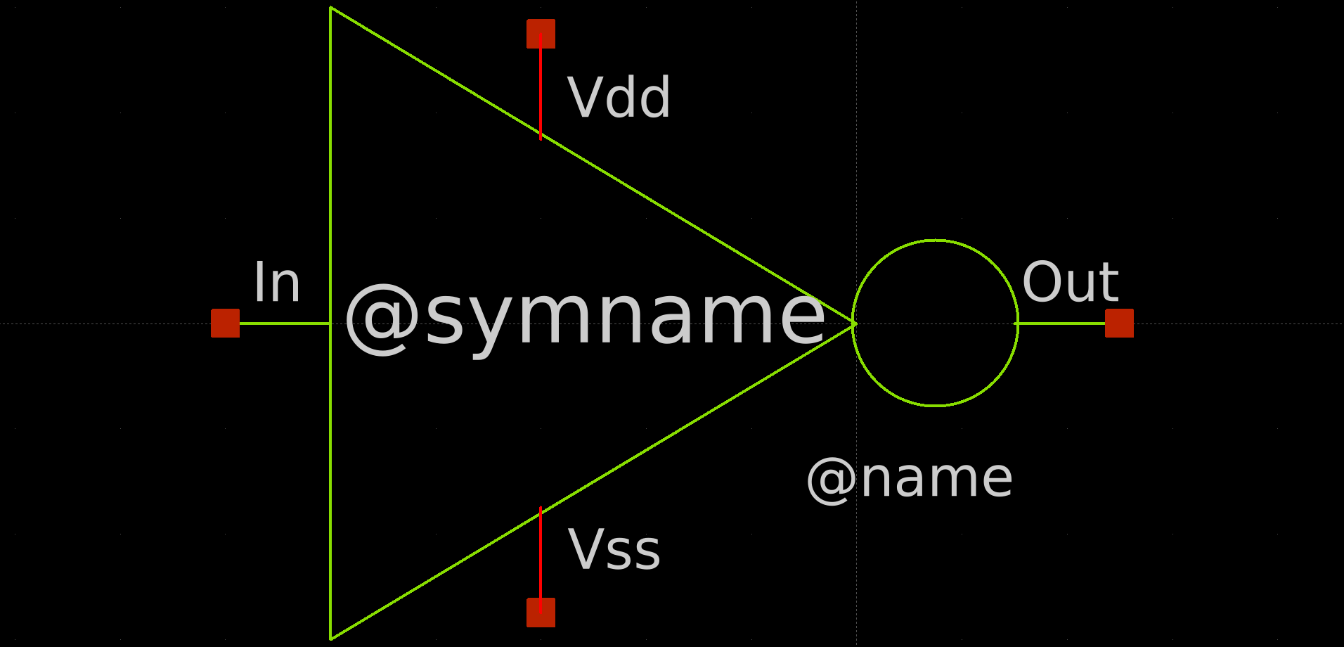
At the highest level, the inverter is represented by the abstract symbol shown above. This symbol is generated directly from the transistor-level schematic and exposes four terminals:
- In - logic input
- Out - logic output
- Vdd - positive supply rail
- Vss - ground reference
This abstraction allows the inverter to be instantiated repeatedly in higher-level schematics while preserving transistor-accurate behavior underneath.
Transistor-Level CMOS Implementation
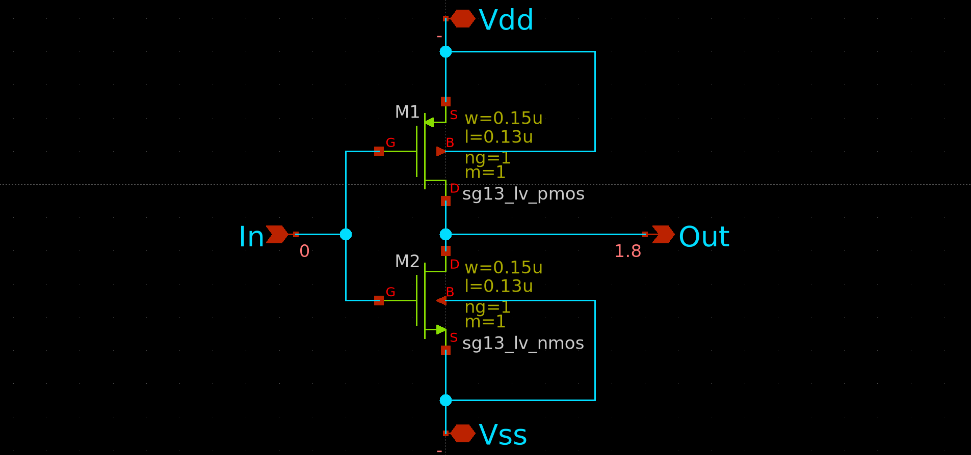
The inverter is implemented using one PMOS and one NMOS device from the IHP SG13 low-voltage library:
sg13_lv_pmossg13_lv_nmos
Topology
- PMOS source connected to Vdd
- NMOS source connected to Vss
- Drains shorted together to form Out
- Gates shorted together to form In
- Bulk terminals tied to their respective sources
This topology ensures zero static power consumption in steady-state logic levels.
Device Dimensions
Both transistors use minimum geometry:
Although symmetric sizing is used here for clarity, production standard cells typically upsize PMOS devices to compensate for reduced hole mobility:
DC Testbench Configuration
To characterize the inverter, a DC sweep testbench is constructed with:
-
Supply voltage:
-
Input sweep:
-
Temperature:
The SPICE control block performs a linear sweep of the input voltage:
dc Vin 0 1.8 1mThis produces the inverter's voltage transfer characteristic (VTC).
DC Transfer Characteristic and Operating Regions
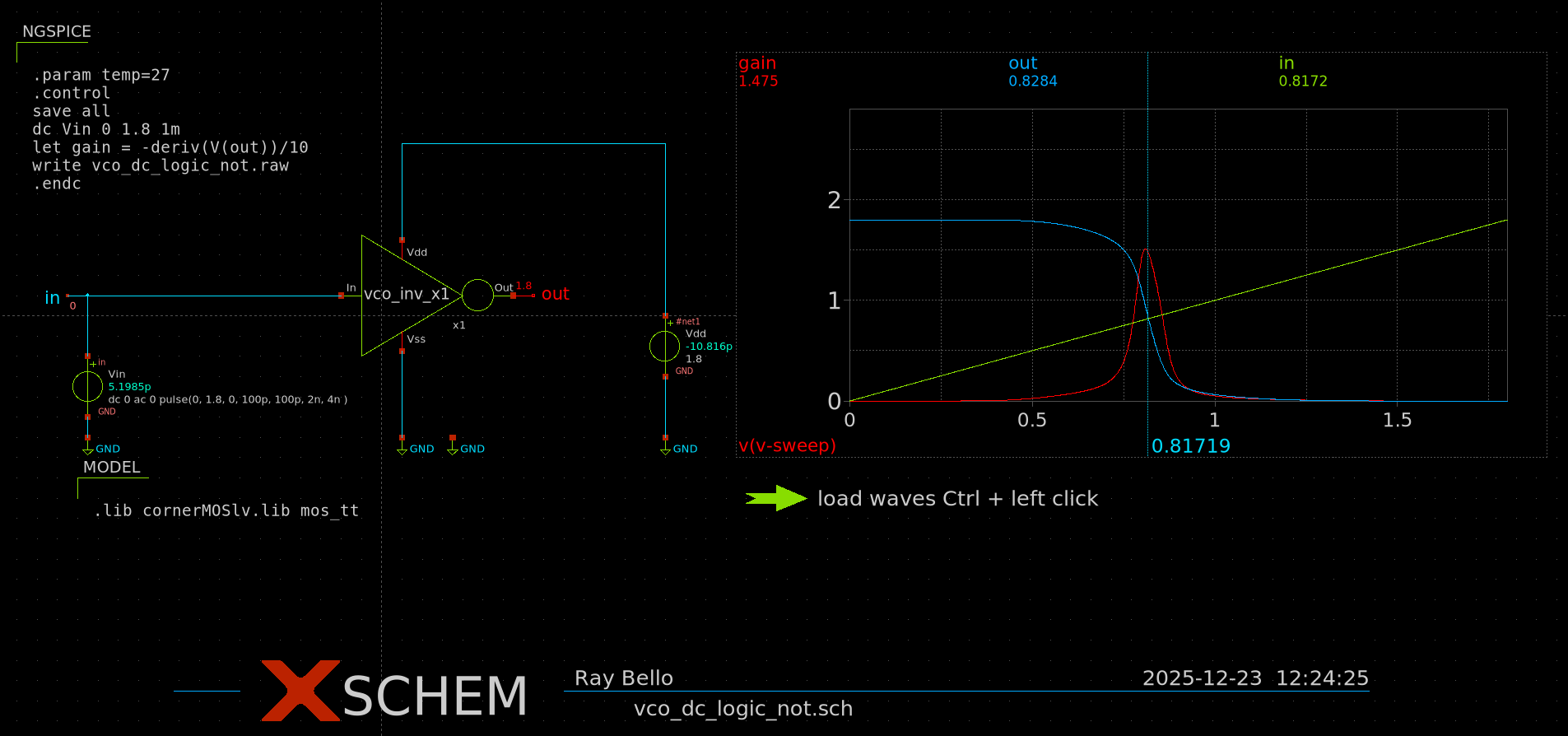
The resulting plot shows:
- Input voltage (green)
- Output voltage (blue)
- Small-signal gain (red)
The inverter behavior can be divided into three operating regions.
Region 1: Low Input Voltage
- NMOS: cutoff
- PMOS: strong inversion
- Output:
This corresponds to a logic high output.
Region 2: Switching Threshold
At the switching point , both transistors conduct simultaneously and the output transitions sharply.
The switching threshold is defined by current equality:
Using long-channel square-law approximations:
From the simulation:
This value matches the cursor location in the plotted transfer curve.
Region 3: High Input Voltage
- NMOS: strong inversion
- PMOS: cutoff
- Output:
This corresponds to a logic low output.
Small-Signal Gain Analysis
The inverter gain is defined as:
Numerically extracted in SPICE using:
let gain = -deriv(v(out))From the plot:
This relatively low gain reflects:
- Minimum-sized devices
- Short-channel effects
- Limited output resistance
Nevertheless, gain greater than unity ensures regenerative switching, which is sufficient for digital logic.
Relevance to TinyTapeout and SG13
This inverter serves as a technology sanity check when working with IHP SG13:
- Confirms correct PDK installation
- Verifies transistor models
- Establishes baseline switching behavior
- Provides a reusable primitive for digital and mixed-signal blocks
Every standard cell ultimately reduces to variations of this structure.
Toolchain Summary (Mac)
git clone --depth=1 https://github.com/iic-jku/iic-osic-tools.git
./start_x.shSwitch PDKs easily:
sak-pdk ihp-sg13g2